EDA Tools
Electronic design automation (EDA) also referred to as electronic computer-aided design (ECAD) is a software tool to design electronic circuits. The software tool generally consists of a design flow to design and analyze the electronic circuit.
Before EDA tools developed, circuit designers used to depend on manually drawing the circuit on a paper or some geometric software to design a circuit. In 1970, circuit developers started to automate the design using software. In 1980, with introduction of VLSI (Very Large Scale Integration), programming languages came into the picture to compile an electronic design. Later, design verification tools and simulation tools are developed to design complex integrated circuits. In 1981, when the beginning of the EDA tools as an industry has actually happened, companies like Hewlett-Packard, Tektronix, and Intel have started using EDA tools internally. This was also the time when companies like Daisy Systems, Mentor Graphics, and Valid Logic Systems were founded. In 1981 itself hardware description language VHDL came into existence. In 1986, another hardware description language Verilog was developed. Later simulators to support these languages quickly developed and in a few more years, back-ends were developed to perform logic synthesis.
As described above, EDA tools generally follow a flow. The design flow can be divided into two designs, digital design and analog design. In digital design a circuit is described using a hardware description language, followed by simulation of circuit design, synthesis, place & route and post layout simulation. In analog design, a circuit is captured, followed by simulation, physical design, layout extraction and post layout simulation. The combined layouts of digital and analog designs are used in a manufacturing facility to produce an electronic chip.
Some of the advantages of EDA tools are minimizing time in designing complex ICs, eliminating manufacturing errors, reducing manufacturing costs, optimizing the IC design and simplicity of usage etc.
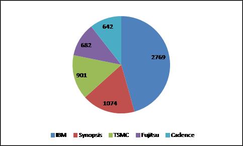
EDA tools IP market also growing steadily all around, as we can see from the patent publication trend from the graph. We can also see that IBM is ruling the IP market followed by Synopsis, TSMC, Fujitsu and Cadence.
(Patent publication trend in EDA domain)
(Top patent assignees in EDA domain)
Although EDA tools offer lot of opportunities to design variety of electronic chips, there are disadvantages too. EDA tools are expensive, many of the tools are not easy to install on a computer system. Many of the tools are not user friendly enough to learn, and there are not many experts available to teach the EDA tools. While the tools available in colleges are good, however, lack of experts to teach the tool, the students are not continuing in EDA domain, rather they are moving into other domains, such as software. If we educate the students about the EDA tools in their early education levels, and if the EDA tools are made cost effective, we can see more students in EDA domain, creating more expertise and better growth in the EDA domain.
